English narration · English + 中文 subtitles burned in · การบรรยายภาษาอังกฤษ · คำบรรยายภาษาอังกฤษ + 中文 ลอยตัวบนภาพ
4.1
Von Neumann architecture · สถาปัตยกรรม Von Neumann
Syllabus · หลักสูตร
English
Candidates should be able to:
Notes and guidance
Show understanding of the basic Von Neumann model for a computer system and the stored program concept
Show understanding of the purpose and role of registers, including the difference between general purpose and special purpose registers
Special purpose registers including: • Program Counter (PC) • Memory Data Register (MDR) • Memory Address Register (MAR) • The Accumulator (ACC) • Index Register (IX) • Current Instruction Register (CIR) • Status Register
Show understanding of the purpose and roles of the Arithmetic and Logic Unit (ALU), Control Unit (CU) and system clock, Immediate Access Store (IAS)
Show understanding of how data are transferred between various components of the computer system using the address bus, data bus and control bus
Show understanding of how factors contribute to the performance of the computer system
Including: • processor type and number of cores • the bus width • clock speed • cache memory
Understand how different ports provide connection to peripheral devices
Including connection to: • Universal Serial Bus (USB) • High Definition Multimedia Interface (HDMI) • Video Graphics Array (VGA)
Describe the stages of the Fetch-Execute (F-E) cycle
Describe and use 'register transfer' notation to describe the F-E cycle
Show understanding of the purpose of interrupts
Including: • possible causes of interrupts • applications of interrupts • use of an Interrupt Service Routine (ISR) • when interrupts are detected during the fetch-execute cycle • how interrupts are handled
ไทย
ผู้เข้าสอบควรสามารถ:
หมายเหตุและคำแนะนำ
แสดงความเข้าใจในโมเดลพื้นฐานของ Von Neumann สำหรับระบบคอมพิวเตอร์และแนวคิด โปรแกรมที่เก็บไว้
Tap the parts of a Von Neumann computer · แตะส่วนประกอบของคอมพิวเตอร์ Von Neumann
Explore each block. The CPU (control unit, ALU, registers) talks to a single main memory over the buses — and that one shared memory for instructions AND data is the Von Neumann idea. · สำรวจแต่ละบล็อก CPU (หน่วยควบคุม, ALU, รีจิสเตอร์) สื่อสารกับหน่วยความจำหลักเพียงแห่งเดียวผ่านบัส — และหน่วยความจำร่วมกันนี้สำหรับคำสั่ง AND ข้อมูลคือแนวคิดของ Von Neumann
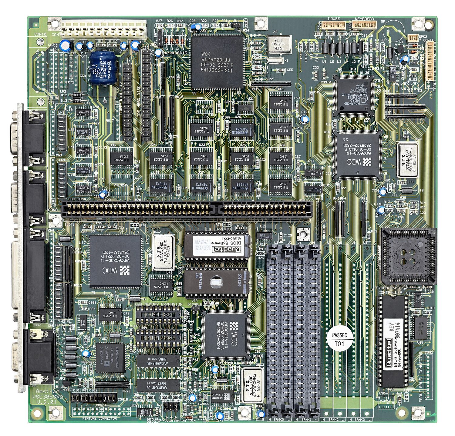
All of these parts sit inside one small chip. The diagram later in this section shows how they connect; the photo below shows the real thing.
Arithmetic and Logic Unit (ALU)
The ALU 算术逻辑单元 does the arithmetic (add, subtract, …) and logic (AND, OR, comparisons). It takes operands from registers 寄存器 and puts results back in a register.
Control Unit (CU)
The control unit 控制单元decodes each instruction and sends the control signals to carry it out — opening data paths, telling the ALU what to do, and controlling memory reads and writes.
System clock
The clock sends a steady stream of pulses that keep the CPU in step. Each instruction takes a fixed number of cycles, and the clock speed 时钟频率 (e.g. 3.8 GHz) is one factor in performance.
"Explain how the CU and the system clock work together": the clock emits pulses at a fixed frequency; the control unit uses each pulse to move the fetch-execute cycle on by one step, sending its control signals in time with the pulses, so every part of the processor changes state together. A faster clock means more steps per second, up to the point where the circuits cannot settle between pulses.
Registers
Registers are tiny, very fast stores inside the CPU. The special purpose registers 专用寄存器 each have a fixed job in the cycle:
Program Counter 程序计数器 (PC) — the address of the next instruction.
Memory Address Register 内存地址寄存器 (MAR) — the address being read or written.
Memory Data Register 内存数据寄存器 (MDR) — the data going to or from memory.
Current Instruction Register 当前指令寄存器 (CIR) — the instruction being decoded.
Accumulator 累加器 (ACC) — the value the ALU is working on.
Status Register 状态寄存器 — holds flags 标志 (carry, zero, negative, overflow) used by branches. Each flag is one bit, set or cleared by the ALU after an operation: the zero flag after a comparison that matched, the carry flag when an addition overflowed the register, the negative flag when a result is negative. A conditional jump reads the flags to decide whether to branch, and an overflow flag can raise an interrupt.
Index Register 变址寄存器 — an offset added to an address in indexed addressing; incrementing it steps through an array one element at a time.
The "complete the table describing the role of each register" question wants one precise sentence per register in these terms: the PC holds the address of the next instruction to be fetched; the MAR holds the address of the location being read from or written to; the MDR holds the data or instruction just read from, or about to be written to, that location; the CIR holds the instruction currently being decoded and executed; the ACC holds the result of the last arithmetic or logic operation.
General-purpose registers 通用寄存器 are used by the programmer for temporary values during a calculation. Movements of data between registers and memory are written in register transfer 寄存器传送 notation — e.g. MAR ← [PC] ("copy the contents of PC into MAR").
CPU สมัยใหม่: โปรเซสเซอร์ทั้งหมดคือชิปเล็กชิ้นหนึ่ง (เห็นจากด้านล่าง แสดงจุดสัมผัส)ซ็อกเก็ต CPU ที่ตรงกับบนเมนบอร์ด: จุดสัมผัสของชิกดันลงบนหมุดเหล่านี้
คำถาม "เติมตารางที่อธิบายบทบาทของแต่ละ register" ต้องการประโยคที่แม่นยำหนึ่งประโยคต่อregister ใน Terms เหล่านี้: PC เก็บที่อยู่ของคำสั่งถัดไปที่จะดึง; MAR เก็บที่อยู่ของตำแหน่งที่กำลังอ่านหรือเขียน; MDR เก็บข้อมูลหรือคำสั่งที่เพิ่งอ่านจากหรือกำลังจะเขียนไปยังตำแหน่งนั้น; CIR เก็บคำสั่งที่กำลัง decode และ run อยู่; ACC เก็บผลลัพธ์ของการดำเนินการ arithmetic หรือ logic ครั้งล่าสุด.
รีจิสเตอร์อเนกประสงค์ ใช้โดยโปรแกรมเมอร์สำหรับค่าชั่วคราวระหว่างการคำนวณ การถ่ายโอนข้อมูลระหว่างรีจิสเตอร์และหน่วยความจำเขียนในรูปสัญลักษณ์ register transfer — เช่น MAR ← [PC] ("คัดลอกเนื้อหาของ PC ลงใน MAR").
CPUVon Neumann: รีจิสเตอร์, หน่วยควบคุม และ ALU เชื่อมต่อกันด้วยบัส
What affects performance · ปัจจัยที่มีผลต่อประสิทธิภาพการทำงาน
English
clock speed — more cycles per second.
number of cores 核心 — a multi-core CPU runs several threads at once.
word size 字长 — a 64-bit CPU handles 64-bit chunks per cycle and can address far more memory than a 32-bit one.
amount of RAM 随机存取存储器 — more RAM holds more of the working set; too little forces the OS to page 页 to disk.
cache memory 高速缓存 size — more cache cuts average memory access time.
secondary storage 辅助存储器 type — an SSD loads programs far faster than an HDD.
bus width and speed — wider/faster buses move data more quickly.
Match the specs to the workload: a quad-core beats a dual-core on parallel work, but higher per-core speed wins on single-threaded work.
Each factor is a two-mark answer with a reason attached:
More cores: each core can fetch and execute its own instruction at the same time, so several programs, or the threads of one program, run in parallel. But a program must be written to use more than one core, so doubling the cores does not double the speed.
Higher clock speed: more fetch-execute cycles per second, so more instructions per second; the limit is the heat produced.
Wider bus: a wider data bus moves more bits in each transfer, so fewer transfers are needed for the same data; a wider address bus can address more memory locations.
Cache memory: a small, fast memory inside or next to the processor that keeps the instructions and data used most recently or most often. Reading them from cache is much faster than from RAM, so the processor spends less time waiting.
"Explain why the new computer performs better" is answered by comparing the two specifications line by line: a higher clock speed executes more instructions per second, more cores run more tasks at once, more cache means fewer slow accesses to RAM, and more RAM means fewer transfers to disk.
Different ports use different signals, so an HDMI cable will not fit a USB socket. USB-C is unusual in carrying video, data and power.
"Explain how the computer connects to the monitor through HDMI": the HDMI port sends the video and the audio as one digital signal down a single cable, so no conversion to analogue is needed and the picture is not degraded; the cable carries high-definition resolutions and the monitor's own port decodes the signal. A USB device is plug-and-play: when it is connected the computer detects it, identifies it, loads or installs the driver it needs, and can supply it with power, all without a restart.
The CPU repeats the fetch-execute cycle 取指-执行周期, one run per machine instruction.
Fetch
the PC's address is copied to the MAR.
the PC is incremented to point to the next instruction.
a read signal goes over the control bus.
memory puts the instruction on the data bus.
it is copied into the MDR, then into the CIR.
The exam asks for these steps in register transfer notation 寄存器传送记法, where [X] means the contents of register X and [[MAR]] means the contents of the memory location whose address is in the MAR:
The order matters: the PC is incremented straight after its address has been copied, so that a jump executed later can still overwrite it. During execution the same notation describes each instruction; for LDD 200, for example, MAR ← 200, MDR ← [[MAR]], ACC ← [MDR].
Decode
The CU decodes the instruction in the CIR — what operation, and which operands or addresses.
Execute
The CU carries it out: arithmetic/logic goes to the ALU (result to the ACC); a load/store moves data between memory and a register; a branch changes the PC. Then the cycle repeats.
ไทย
CPU ทำซ้ำ รอบ fetch-execute — รันหนึ่งครั้งต่อคำสั่งเครื่องหนึ่ง
Fetch
ที่อยู่ของ PC ถูกคัดลอกไปยัง MAR
PC ถูก increment เพื่อชี้ไปที่คำสั่งถัดไป
สัญญาณ read ส่งผ่านบัสควบคุม
หน่วยความจำวางคำสั่งลงบนบัสข้อมูล
คัดลอกเข้าไปใน MDR จากนั้นเข้าสู่ CIR
ข้อสอบถามขั้นตอนเหล่านี้ในรูปแบบ register transfer notation โดยที่ [X] หมายถึงเนื้อหาของรีจิสเตอร์ X และ [[MAR]] หมายถึงเนื้อหาของตำแหน่งหน่วยความจำwhose address อยู่ใน MAR:
MAR ← [PC]          the address of the next instruction goes to the MAR
PC  ← [PC] + 1      the PC now points to the following instruction
MDR ← [[MAR]]       the instruction at that address is read into the MDR
CIR ← [MDR]         the instruction is copied into the CIR for decoding
ลำดับมีความสำคัญ: PC จะถูก increment ทันทีหลังจากที่อยู่ของมันถูกคัดลอก เพื่อให้การ jump ที่เกิดขึ้นในภายหลังสามารถแทนที่ค่า PC นั้นได้ ระหว่างการ execute สัญลักษณ์เดียวกันนี้จะใช้อธิบายแต่ละคำสั่ง; สำหรับ LDD 200 ตัวอย่างเช่น MAR ← 200, MDR ← [[MAR]], ACC ← [MDR]
การถ่ายโอนรีจิสเตอร์ในรอบ fetch: PC → MAR → หน่วยความจำ → MDR → CIR โดยมีการ increment PC
Decode
CU ตีความคำสั่งใน CIR — ว่าเป็นการดำเนินการใด และใช้ operand หรือที่อยู่ข้อมูลใด
การดำเนินการ (Execute)
CU ดำเนินการตามนั้น: การคำนวณทางคณิตศาสตร์/ตรรกะจะถูกส่งไปยัง ALU (ผลลัพธ์ไป ACC); การโหลด/จัดเก็บจะย้ายข้อมูลระหว่างหน่วยความจำและรีจิสเตอร์; การกระโดดจะเปลี่ยนค่า PC จากนั้นรอบการทำงานจะวนซ้ำอีกครั้ง
Tap round the loop the CPU repeats billions of times a second. Watch how fetch uses the PC/MAR/MDR/CIR registers, then decode and execute act on what was fetched. · แตะวนรอบที่ CPU ทำซ้ำหลายพันล้านครั้งต่อวินาที ดูว่า fetch ใช้รีจิสเตอร์ PC/MAR/MDR/CIR อย่างไร แล้ว decode และ execute ทำงานกับสิ่งที่ถูกดึงมา
Explore · สำรวจ
The fetch–execute cycle · 取指-执行周期
Step through how the CPU runs one instruction — fetch it from memory, decode it, then execute it, over and over. · 逐步演示CPU如何运行一条指令——从内存中fetch,decode,然后execute,周而复始。
register transfer notation/ˈredʒɪstə ˈtrænsfɜː nəʊˈteɪʃn/
Programming Transfer Notation
interrupt service routine/ˈɪntərʌpt ˈsɜːvɪs ruːˈtiːn/
Interrupt Service Routine
4.1
Interrupts
English
An interrupt 中断 is a signal that pauses the normal cycle so the CPU can handle an urgent event (a key press, a packet arriving, a hardware fault, division by zero, the OS timer).
Handling one:
finish the current instruction.
save the state (PC and registers).
load the address of the interrupt service routine 中断服务程序 (ISR) into the PC and run it.
the ISR handles the event.
restore the saved state and carry on.
Interrupts let the system respond promptly without the CPU constantly checking devices, and are how the OS multitasks.
"Explain how an interrupt from an input device is detected and handled in the F-E cycle" is a four-mark answer with these points: the device sends an interrupt signal that sets the interrupt flag in the interrupt register 中断寄存器; the processor checks that register at the end of every fetch-execute cycle, after the current instruction has finished executing; if a flag is set and the interrupt has a higher priority than the current task, the contents of the PC and the other registers are saved onto the stack 栈; the address of the interrupt service routine is loaded into the PC and the routine runs; when it finishes, the saved values are restored from the stack and the interrupted program continues from where it stopped.
Causes worth naming: a hardware interrupt from a device (a key pressed, a printer buffer empty, a network packet arriving), a software interrupt from a fault (division by zero, an illegal instruction, arithmetic overflow), a timer interrupt from the operating system marking the end of a time slice, and a power failure warning.
Show understanding of the relationship between assembly language and machine code
Describe the different stages of the assembly process for a two-pass assembler
Apply the two-pass assembler process to a given simple assembly language program
Trace a given simple assembly language program
Show understanding that a set of instructions are grouped
Including the following groups: • Data movement • Input and output of data • Arithmetic operations • Unconditional and conditional instructions • Compare instructions
Show understanding of and be able to use different modes of addressing
Including immediate, direct, indirect, indexed, relative
Source: Cambridge International syllabus · แหล่งที่มา: หลักสูตร Cambridge International
English
The CPU actually runs machine code 机器码 — bit patterns, specific to one architecture. Assembly language 汇编语言 is a readable form, with one instruction per machine instruction, written using mnemonics 助记符 like LDD, ADD, JMP. An assembler 汇编器 translates it to machine code.
Two-pass assembler
A two-pass assembler reads the source twice:
pass 1 builds a symbol table 符号表: each time a label 标签 (like LOOP:) appears, record its address; no code yet.
pass 2 generates code: translate each instruction, and when one refers to a label (like JMP LOOP), look up its address in the symbol table.
Two passes handle forward references 前向引用 (a jump to a label defined later).
Worked example. Apply the two-pass process to this program, whose first instruction is stored at address 100.
Pass 1 reads each line, counts the address it will occupy, and records every label in the symbol table: LOOP = 101 (the DEC line) and COUNT = 105 (the data line). No code is produced. Pass 2 reads the program again and translates each line into machine code, replacing each mnemonic by its opcode 操作码 and each symbolic address by the number from the symbol table: LDD COUNT becomes the opcode for LDD with operand 操作数 105, and JPN LOOP becomes the opcode for JPN with operand 101. The jump back to LOOP could have been resolved in one pass, but a jump forward to a label not yet seen could not, which is why the assembler makes two.
Example instruction set
Cambridge uses a small generic set, printed in the paper's reference table, with one general-purpose register, the accumulator (ACC), and an index register (IX). An operand written #n is a denary number, Bn a binary number and &n a hexadecimal number; <address> is a location number or a label.
Group
Instruction
What it does
Data movement
LDM #n
load the number n into ACC (immediate)
LDD <address>
load the contents of the address into ACC (direct)
LDI <address>
the address holds another address; load the contents of that one into ACC (indirect)
LDX <address>
add IX to the address and load the contents of the result into ACC (indexed)
LDR #n
load the number n into IX
MOV <register>
copy ACC into the named register (IX)
STO <address>
store the contents of ACC at the address
Input and output
IN
read a key press and put its ASCII code in ACC
OUT
output the character whose ASCII code is in ACC
Arithmetic
ADD <address> / ADD #n
add the contents of the address, or the number, to ACC
SUB <address> / SUB #n
subtract from ACC
INC <register> / DEC <register>
add 1 to, or subtract 1 from, ACC or IX
Compare
CMP <address> / CMP #n
compare ACC with the contents of the address, or with n, and set the flag
CMI <address>
compare ACC with the contents of the address held at the address (indirect)
Jump
JMP <address>
jump to the address unconditionally
JPE <address> / JPN <address>
jump if the last compare was equal / not equal
Bit manipulation
AND, OR, XOR with #n, Bn, &n or <address>
bitwise operation on ACC
LSL #n / LSR #n
shift ACC logically n places left or right
END
end the program
The "assembly language instructions are grouped" question wants the group names, and an instruction from each: data movement, input and output, arithmetic, unconditional and conditional jumps, compare, and bit manipulation.
How a two-pass assembler works · วิธีการทำงานของแอสsembl์แบบสองรอบ
Step through it. The assembler reads your code twice: pass 1 just finds where every label lives, so pass 2 can fill in the addresses — that is how a jump to a label defined later still works. · ลองเดินตามกระบวนการดู แอสsembl์จะอ่านโค้ดของคุณสองครั้ง: รอบ 1 จะหาตำแหน่งของแต่ละฉลาก (label) เพื่อให้อรอบ 2 สามารถกรอกที่อยู่ได้ — นั่นคือเหตุผลว่าทำไมการกระโดดไปยังฉลากที่นิยาม ภายหลัง จึงยังทำงานได้
The addressing mode 寻址方式 (the modes of addressing) says how the CPU finds the operand:
immediate addressing 立即寻址 — the operand is the value in the instruction. LDM #10 loads 10.
direct addressing 直接寻址 — the instruction holds an address; the operand is the value there. LDD 200.
indirect addressing 间接寻址 — the instruction holds an address that holds another address, which is the data. LDI 200.
indexed addressing 变址寻址 — effective address is address + index register; used for arrays. LDX 100 with IR = 5 reads address 105.
(Relative addressing 相对寻址 gives the address as an offset from the PC — used for jumps.)
Worked example. Memory holds: location 200 = 250, location 250 = 99, location 105 = 7. The index register holds 5. What is in the accumulator after each of LDM #200, LDD 200, LDI 200 and LDX 100? Follow how far each mode has to look. LDM #200 is immediate - the operand is the number written in the instruction, so the accumulator holds 200. LDD 200 is direct - go to location 200 and take what is there: 250. LDI 200 is indirect - location 200 holds 250, which is another address, so go on to location 250: 99. LDX 100 is indexed - add the index register to the address, $100 + 5 = 105$, and read location 105: 7. Count the hops to keep them apart: immediate 0, direct 1, indirect 2, indexed 1 (once the index has been added).
ไทย
โหมดการเข้าถึง (หรือ modes of addressing) บอกวิธีการที่ CPU หา operands:
Tracing an assembly program · การติดตามโปรแกรมอัสsembly
English
To trace it: make a table with columns for the PC, ACC, index register, each variable and any flags. Step through the instructions, updating the table after each; follow branches when they change the PC; stop at END. A common pattern is a loop over an array using indexed addressing.
Worked example. Trace this program. Address 200 holds 5 and address 201 holds 0.
Write one row for each instruction executed, filling in only the columns that change:
Instruction
ACC
200
201
Output
start
5
0
LDD 200
5
CMP #0
JPE 108
not taken
OUT
character with code 5
DEC ACC
4
STO 200
4
LDD 201
0
JMP 100
LDD 200
4
and so on, until LDD 200 loads 0, the compare sets the equal flag, JPE 108 is taken and the program ends. Three things the examiner checks: a CMP changes no register, only a flag; a jump not taken still counts as executed; and OUT outputs a character, so it goes in the output column, not the ACC column. "State the effect of changing LDD 10 to LDM #10": the ACC would hold the number 10 instead of the contents of address 10.
Logical, arithmetic and cyclic Left shift, right shift
Show understanding of how bit manipulation can be used to monitor/control a device
Carry out bit manipulation operations Test and set a bit (using bit masking)
Instruction Label | Opcode | Operand
Explanation
AND #n / Bn / &n
Bitwise AND operation of the contents of ACC with the operand
AND
Bitwise AND operation of the contents of ACC with the contents of
XOR #n / Bn / &n
Bitwise XOR operation of the contents of ACC with the operand
XOR
Bitwise XOR operation of the contents of ACC with the contents of
OR #n / Bn / &n
Bitwise OR operation of the contents of ACC with the operand
OR
Bitwise OR operation of the contents of ACC with the contents of
LSL #n
Bits in ACC are shifted logically n places to the left. Zeros are introduced on the right hand end
LSR #n
Bits in ACC are shifted logically n places to the right. Zeros are introduced on the left hand end
Labels an instruction
Gives a symbolic address
All questions will assume there is only one general purpose register available (Accumulator) ACC denotes Accumulator IX denotes Index Register can be an absolute or symbolic address # denotes a denary number, e.g. #123 B denotes a binary number, e.g. B01001010 & denotes a hexadecimal number, e.g. &4A
การดำเนินการ OR แบบบิตต่อบิตของเนื้อหาใน ACC กับ operand
OR
การดำเนินการ OR แบบบิตต่อบิตของเนื้อหาใน ACC กับเนื้อหาใน
LSL #n
บิตใน ACC会被เลื่อนไปทางซ้าย n ตำแหน่งตามหลักตรรกะ จะเพิ่มค่าศูนย์เข้าไปที่ด้านขวา
LSR #n
บิตใน ACC会被เลื่อนไปทางขวา n ตำแหน่งตามหลักตรรกะ จะเพิ่มค่าศูนย์เข้าไปที่ด้านซ้าย
ทำเครื่องหมายชื่อตำแหน่งกับคำสั่ง
ให้ที่อยู่เชิงสัญลักษณ์
ข้อคำถามทั้งหมดจะสมมติว่ามีรีจิสเตอร์ใช้งานทั่วไปเพียงหนึ่งตัว (Accumulator) ACC หมายถึง Accumulator IX หมายถึง Index Register อาจเป็นที่อยู่แบบabsoluteหรือเชิงสัญลักษณ์ # หมายถึงตัวเลขฐานสิบ เช่น #123 B หมายถึงตัวเลขฐานสอง เช่น B01001010 & หมายถึงตัวเลขฐานหก عشر เช่น &4A
Source: Cambridge International syllabus · แหล่งที่มา: หลักสูตร Cambridge International
English
A logical shift 逻辑移位 moves all the bits left or right by some places, filling new positions with 0.
left shift by 1 (LSL #1) — bits move left, a 0 enters on the right; for an unsigned number this is × 2.
right shift by 1 (LSR #1) — bits move right, a 0 enters on the left; for an unsigned number this is integer ÷ 2.
Shifting by $n$ places multiplies or divides by $2^{n}$. Example: 00001011 (11) LSL #1 → 00010110 (22).
Bits shifted off the end are lost, so the multiplication is only correct while they were zeros. LSL #2 on the two's-complement integer 11001010 gives 00101000: the two 1s that fell off the left are gone, the sign bit has changed, and the result is no longer four times the original.
An arithmetic right shift keeps the sign bit so a negative signed number stays negative. A cyclic shift 循环移位 (rotate) feeds the bit that drops off one end back in at the other end, so no bits are lost.
"Show the result of an arithmetic right shift of 3 places on 10011110": copy the sign bit into each vacated place, 11110011. The same shift on 01011100 gives 00001011. A cyclic left shift of 1 on 10000110 gives 00001101: the leading 1 reappears on the right.
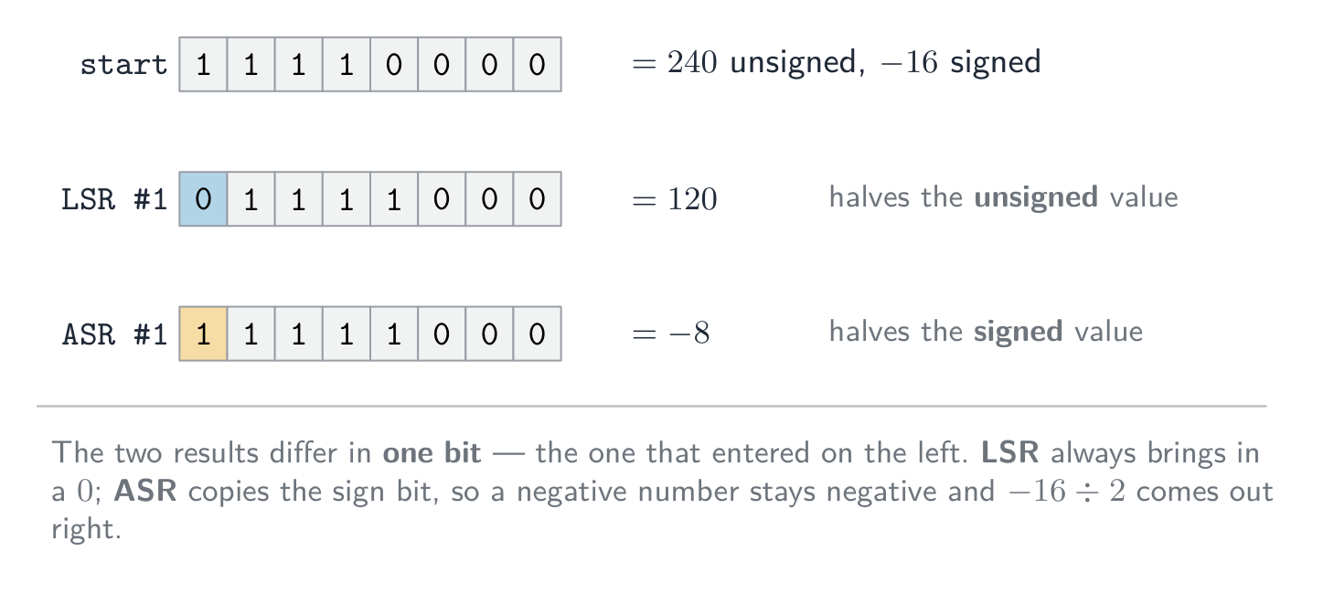
The difference between the two right shifts is a single bit. Take 11110000, which is 240 read as unsigned and $-16$ read as signed. LSR #1 brings in a 0 and gives 01111000$= 120$, which is the correct half of 240. ASR #1 copies the sign bit instead and gives 11111000$= -8$, which is the correct half of $-16$. Neither is wrong — each halves the value under one reading.
Bit manipulation for monitoring/control
Embedded devices often use one bit 位 of a register per signal (e.g. bit $n$ = LED $n$). Using a mask 掩码 — bit masking — you can:
set bit $n$: R = R OR a mask with bit $n$ set.
clear bit $n$: R = R AND a mask with bit $n$ clear and the rest set.
toggle bit $n$: R = R XOR a mask with bit $n$ set.
test bit $n$: R AND the mask, then check if the result is non-zero.
Bit manipulation is fast, uses little memory, and lets one byte hold up to 8 on/off states.
In the exam's instruction set these are AND, OR and XOR with a mask written as a denary, binary or hexadecimal operand. With the ACC holding 10101100:
Instruction
Mask
Result in ACC
Effect
AND B00001111
00001111
00001100
keeps only the low four bits (clears the others)
OR #1
00000001
10101101
sets the least significant bit, leaving the rest unchanged
XOR &FF
11111111
01010011
inverts every bit
AND B00001000 then CMP #0
00001000
00001000
tests bit 3: the compare is not equal, so bit 3 was set
LSL #2
10110000
shifts left two places, losing the top two bits
LSR #3
00010101
shifts right three places, zeros entering on the left
"Write the instruction that sets the least significant bit to 1 and leaves the others unchanged": OR #1, or OR B00000001. To clear a bit use AND with a mask that has a 0 in that place and 1s elsewhere; to test a bit, AND with a mask that has a 1 only in that place, then compare the result with zero. In a monitoring device, one bit of a register per sensor lets a single AND check whether a particular sensor is on, and one OR switches an actuator's control bit on without disturbing the others.
"เขียนคำสั่งที่ตั้งค่าบิตที่มีนัยสำคัญต่ำสุดให้เป็น 1 และทิ้งส่วนอื่นไว้ไม่เปลี่ยน": OR #1, หรือ OR B00000001. เพื่อลบค่าบิต ให้ใช้ AND กับมาส์กที่มี 0 ในตำแหน่งนั้นและ 1 ที่อื่นๆ; เพื่อทดสอบบิต, AND กับมาส์กที่มี 1 เพียงตำแหน่งเดียว, แล้วเปรียบเทียบผลลัพธ์กับศูนย์. ในอุปกรณ์ตรวจสอบ, บิตของเรจิสเตอร์หนึ่งบิตต่อเซ็นเซอร์ช่วยให้ AND เดียวสามารถตรวจสอบได้ว่าเซ็นเซอร์ใดเปิดอยู่, และ OR ตัวหนึ่งจะเปิดบิตควบคุมแอค추เอเตอร์โดยไม่รบกวนส่วนอื่น
Explore · สำรวจ
Shift and mask the bits of a byte · เลื่อนและบดบิตของไบต์
Pick an operator and watch each result bit. A left shift (<<) moves every bit up one place (×2); a right shift (>>) moves them down (÷2); AND with a mask clears the bits you don't want. · เลือกตัวดำเนินการและดูผลลัพธ์ของแต่ละบิต การเลื่อนซ้าย (<<) moves every bit up one place (×2); a right shift (>>) จะย้ายลง (÷2); AND กับมาส์กจะลบบิตที่ไม่ต้องการออก
Learn the fetch-execute cycle in register-transfer terms (PC, MAR, MDR, CIR, ACC) and what increments the PC.
Name each register's job; the address bus is one-way, the data bus is two-way.
Distinguish the addressing modes (immediate, direct, indirect, indexed) — a frequent question.
Explain how clock speed, number of cores, cache size and word length affect performance.
For a binary shift, state whether it is logical or arithmetic; a left shift multiplies by 2, a right shift divides by 2.
Common mistakes
Saying the PC holds the current instruction, or the MDR holds an address. The PC holds the address of the next instruction; the MDR holds data or an instruction, never an address.
Leaving the increment of the PC out of the fetch, or putting it after the execute. It happens as soon as the address has been copied to the MAR.
Reading LDD 10 as "load 10". LDD 10 loads the contents of address 10; LDM #10 loads the number 10.
Putting a value in the ACC column for CMP or OUT. A compare sets a flag only; an output goes to the output column.
Saying an interrupt is handled "immediately". The processor finishes the current instruction and checks for interrupts at the end of the cycle.
Using a logical right shift on a negative two's-complement number. Only an arithmetic shift keeps the sign bit.
ไทย
เรียนรู้ รอบดึง-ดำเนินการ ในพจน์การถ่ายโอนเรจิสเตอร์ (PC, MAR, MDR, CIR, ACC) และสิ่งใดเพิ่มค่า PC.
Pick one and the site follows you — notes, papers, videos and practice all open on it. · เลือกหนึ่งตัว และเว็บจะติดตามคุณ — หมายเหตุ, ใบงาน, วิดีโอ และการฝึกฝนจะเปิดอยู่ที่นั้น
Type to search notes, lessons, code, vocabulary and past-paper questions across every subject. · พิมพ์เพื่อค้นหาบันทึก, บทเรียน, โค้ด, คำศัพท์ และคำถามข้อสอบเก่าในทุกวิชา