| Candidates should be able to: | Notes and guidance |
|---|---|
| Show understanding of the basic Von Neumann model for a computer system and the stored program concept | |
| Show understanding of the purpose and role of registers, including the difference between general purpose and special purpose registers | Special purpose registers including: • Program Counter (PC) • Memory Data Register (MDR) • Memory Address Register (MAR) • The Accumulator (ACC) • Index Register (IX) • Current Instruction Register (CIR) • Status Register |
| Show understanding of the purpose and roles of the Arithmetic and Logic Unit (ALU), Control Unit (CU) and system clock, Immediate Access Store (IAS) | |
| Show understanding of how data are transferred between various components of the computer system using the address bus, data bus and control bus | |
| Show understanding of how factors contribute to the performance of the computer system | Including: • processor type and number of cores • the bus width • clock speed • cache memory |
| Understand how different ports provide connection to peripheral devices | Including connection to: • Universal Serial Bus (USB) • High Definition Multimedia Interface (HDMI) • Video Graphics Array (VGA) |
| Describe the stages of the Fetch-Execute (F-E) cycle | Describe and use 'register transfer' notation to describe the F-E cycle |
| Show understanding of the purpose of interrupts | Including: • possible causes of interrupts • applications of interrupts • use of an Interrupt Service Routine (ISR) • when interrupts are detected during the fetch-execute cycle • how interrupts are handled |
Processor Fundamentals
A-Level Computer Science · Topic 4
4.1
Von Neumann architecture
Syllabus
Source: Cambridge International syllabus
The Von Neumann architecture 冯·诺依曼体系结构 underlies almost every general-purpose computer:
- a single memory — the Immediate Access Store 立即存取存储器 (IAS) — holds both program instructions and data (the stored program 存储程序 concept).
- a processor 处理器 (CPU) fetches instructions from memory and runs them one at a time.
- instructions run in order unless a branch changes the flow.
The stored-program idea is what makes a computer flexible: change the program and you change what it does, with no rewiring.
Explore
Tap the parts of a Von Neumann computer
Explore each block. The CPU (control unit, ALU, registers) talks to a single main memory over the buses — and that one shared memory for instructions AND data is the Von Neumann idea.
Vocabulary
Train
| English | Chinese | Pinyin |
|---|---|---|
| Von Neumann architecture | 冯·诺依曼体系结构 | féng · nuò yī màn tǐ xì jié gòu |
| Immediate Access Store | 立即存取存储器 | lì jí cún qǔ cún chǔ qì |
| stored program | 存储程序 | cún chǔ chéng xù |
| processor | 处理器 | chǔ lǐ qì |
| RAM | 随机存取存储器 | suí jī cún qǔ cún chǔ qì |
4.1
The CPU's main parts

All of these parts sit inside one small chip. The diagram later in this section shows how they connect; the photo below shows the real thing.

Arithmetic and Logic Unit (ALU)
The ALU 算术逻辑单元 does the arithmetic (add, subtract, …) and logic (AND, OR, comparisons). It takes operands from registers 寄存器 and puts results back in a register.
Control Unit (CU)
The control unit 控制单元 decodes each instruction and sends the control signals to carry it out — opening data paths, telling the ALU what to do, and controlling memory reads and writes.
System clock
The clock sends a steady stream of pulses that keep the CPU in step. Each instruction takes a fixed number of cycles, and the clock speed 时钟频率 (e.g. 3.8 GHz) is one factor in performance.
"Explain how the CU and the system clock work together": the clock emits pulses at a fixed frequency; the control unit uses each pulse to move the fetch-execute cycle on by one step, sending its control signals in time with the pulses, so every part of the processor changes state together. A faster clock means more steps per second, up to the point where the circuits cannot settle between pulses.
Registers
Registers are tiny, very fast stores inside the CPU. The special purpose registers 专用寄存器 each have a fixed job in the cycle:
- Program Counter 程序计数器 (PC) — the address of the next instruction.
- Memory Address Register 内存地址寄存器 (MAR) — the address being read or written.
- Memory Data Register 内存数据寄存器 (MDR) — the data going to or from memory.
- Current Instruction Register 当前指令寄存器 (CIR) — the instruction being decoded.
- Accumulator 累加器 (ACC) — the value the ALU is working on.
- Status Register 状态寄存器 — holds flags 标志 (carry, zero, negative, overflow) used by branches. Each flag is one bit, set or cleared by the ALU after an operation: the zero flag after a comparison that matched, the carry flag when an addition overflowed the register, the negative flag when a result is negative. A conditional jump reads the flags to decide whether to branch, and an overflow flag can raise an interrupt.
- Index Register 变址寄存器 — an offset added to an address in indexed addressing; incrementing it steps through an array one element at a time.
The "complete the table describing the role of each register" question wants one precise sentence per register in these terms: the PC holds the address of the next instruction to be fetched; the MAR holds the address of the location being read from or written to; the MDR holds the data or instruction just read from, or about to be written to, that location; the CIR holds the instruction currently being decoded and executed; the ACC holds the result of the last arithmetic or logic operation.
General-purpose registers 通用寄存器 are used by the programmer for temporary values during a calculation. Movements of data between registers and memory are written in register transfer 寄存器传送 notation — e.g. MAR ← [PC] ("copy the contents of PC into MAR").

Vocabulary
Train
| English | Chinese | Pinyin |
|---|---|---|
| ALU | 算术逻辑单元 | suàn shù luó jí dān yuán |
| registers | 寄存器 | jì cún qì |
| control unit | 控制单元 | kòng zhì dān yuán |
| clock speed | 时钟频率 | shí zhōng pín lǜ |
| special purpose registers | 专用寄存器 | zhuān yòng jì cún qì |
| Program Counter | 程序计数器 | chéng xù jì shù qì |
| Memory Address Register | 内存地址寄存器 | nèi cún dì zhǐ jì cún qì |
| Memory Data Register | 内存数据寄存器 | nèi cún shù jù jì cún qì |
| Current Instruction Register | 当前指令寄存器 | dāng qián zhǐ lìng jì cún qì |
| Accumulator | 累加器 | lěi jiā qì |
| Status Register | 状态寄存器 | zhuàng tài jì cún qì |
| flags | 标志 | biāo zhì |
| Index Register | 变址寄存器 | biàn zhǐ jì cún qì |
| General-purpose registers | 通用寄存器 | tōng yòng jì cún qì |
| register transfer | 寄存器传送 | jì cún qì chuán sòng |
4.1
Buses

Three internal buses 总线 (sets of parallel wires) connect the parts:
- address bus 地址总线 — carries the memory address. One-way (CPU → memory).
- data bus 数据总线 — carries the data. Two-way.
- control bus 控制总线 — carries control signals (read, write, interrupt). Two-way.
An $n$-bit address bus can reach $2^{n}$ memory locations. The data-bus width sets how many bits move per access (often the word size).
Vocabulary
Train
| English | Chinese | Pinyin |
|---|---|---|
| buses | 总线 | zǒng xiàn |
| address bus | 地址总线 | dì zhǐ zǒng xiàn |
| data bus | 数据总线 | shù jù zǒng xiàn |
| control bus | 控制总线 | kòng zhì zǒng xiàn |
4.1
What affects performance
- clock speed — more cycles per second.
- number of cores 核心 — a multi-core CPU runs several threads at once.
- word size 字长 — a 64-bit CPU handles 64-bit chunks per cycle and can address far more memory than a 32-bit one.
- amount of RAM 随机存取存储器 — more RAM holds more of the working set; too little forces the OS to page 页 to disk.
- cache memory 高速缓存 size — more cache cuts average memory access time.
- secondary storage 辅助存储器 type — an SSD loads programs far faster than an HDD.
- bus width and speed — wider/faster buses move data more quickly.
Match the specs to the workload: a quad-core beats a dual-core on parallel work, but higher per-core speed wins on single-threaded work.
Each factor is a two-mark answer with a reason attached:
- More cores: each core can fetch and execute its own instruction at the same time, so several programs, or the threads of one program, run in parallel. But a program must be written to use more than one core, so doubling the cores does not double the speed.
- Higher clock speed: more fetch-execute cycles per second, so more instructions per second; the limit is the heat produced.
- Wider bus: a wider data bus moves more bits in each transfer, so fewer transfers are needed for the same data; a wider address bus can address more memory locations.
- Cache memory: a small, fast memory inside or next to the processor that keeps the instructions and data used most recently or most often. Reading them from cache is much faster than from RAM, so the processor spends less time waiting.
"Explain why the new computer performs better" is answered by comparing the two specifications line by line: a higher clock speed executes more instructions per second, more cores run more tasks at once, more cache means fewer slow accesses to RAM, and more RAM means fewer transfers to disk.
Vocabulary
Train
| English | Chinese | Pinyin |
|---|---|---|
| number of cores | 核心 | hé xīn |
| word size | 字长 | zì zhǎng |
| amount of RAM | 随机存取存储器 | suí jī cún qǔ cún chǔ qì |
| page | 页 | yè |
| cache memory | 高速缓存 | gāo sù huǎn cún |
| secondary storage | 辅助存储器 | fǔ zhù cún chǔ qì |
| cores | 核心 | hé xīn |
4.1
Ports
A port 端口 is a physical socket for connecting a peripheral 外围设备:
- USB (Universal Serial Bus) — general-purpose (keyboards, drives, phones).
- HDMI (High Definition Multimedia Interface) — digital video and audio to a screen.
- VGA (Video Graphics Array) — older analogue video output to a monitor.
- Ethernet (RJ-45) — wired LAN. Audio jacks — headphones/microphone.
Different ports use different signals, so an HDMI cable will not fit a USB socket. USB-C is unusual in carrying video, data and power.
"Explain how the computer connects to the monitor through HDMI": the HDMI port sends the video and the audio as one digital signal down a single cable, so no conversion to analogue is needed and the picture is not degraded; the cable carries high-definition resolutions and the monitor's own port decodes the signal. A USB device is plug-and-play: when it is connected the computer detects it, identifies it, loads or installs the driver it needs, and can supply it with power, all without a restart.
Vocabulary
Train
| English | Chinese | Pinyin |
|---|---|---|
| port | 端口 | duān kǒu |
| peripheral | 外围设备 | wài wéi shè bèi |
4.1
Fetch-Execute cycle

The CPU repeats the fetch-execute cycle 取指-执行周期, one run per machine instruction.
Fetch
- the PC's address is copied to the MAR.
- the PC is incremented to point to the next instruction.
- a read signal goes over the control bus.
- memory puts the instruction on the data bus.
- it is copied into the MDR, then into the CIR.
The exam asks for these steps in register transfer notation 寄存器传送记法, where [X] means the contents of register X and [[MAR]] means the contents of the memory location whose address is in the MAR:
MAR ← [PC]          the address of the next instruction goes to the MAR
PC  ← [PC] + 1      the PC now points to the following instruction
MDR ← [[MAR]]       the instruction at that address is read into the MDR
CIR ← [MDR]         the instruction is copied into the CIR for decoding
The order matters: the PC is incremented straight after its address has been copied, so that a jump executed later can still overwrite it. During execution the same notation describes each instruction; for LDD 200, for example, MAR ← 200, MDR ← [[MAR]], ACC ← [MDR].
Decode
The CU decodes the instruction in the CIR — what operation, and which operands or addresses.
Execute
The CU carries it out: arithmetic/logic goes to the ALU (result to the ACC); a load/store moves data between memory and a register; a branch changes the PC. Then the cycle repeats.

Explore
The fetch-execute cycle
Tap round the loop the CPU repeats billions of times a second. Watch how fetch uses the PC/MAR/MDR/CIR registers, then decode and execute act on what was fetched.
Explore
The fetch–execute cycle
Step through how the CPU runs one instruction — fetch it from memory, decode it, then execute it, over and over.
Vocabulary
Train
| English | Chinese | Pinyin |
|---|---|---|
| fetch-execute cycle | 取指-执行周期 | qǔ zhǐ - zhí xíng zhōu qī |
| register transfer notation | 寄存器传送记法 | jì cún qì chuán sòng jì fǎ |
4.1
Interrupts

An interrupt 中断 is a signal that pauses the normal cycle so the CPU can handle an urgent event (a key press, a packet arriving, a hardware fault, division by zero, the OS timer).
Handling one:
- finish the current instruction.
- save the state (PC and registers).
- load the address of the interrupt service routine 中断服务程序 (ISR) into the PC and run it.
- the ISR handles the event.
- restore the saved state and carry on.
Interrupts let the system respond promptly without the CPU constantly checking devices, and are how the OS multitasks.
"Explain how an interrupt from an input device is detected and handled in the F-E cycle" is a four-mark answer with these points: the device sends an interrupt signal that sets the interrupt flag in the interrupt register 中断寄存器; the processor checks that register at the end of every fetch-execute cycle, after the current instruction has finished executing; if a flag is set and the interrupt has a higher priority than the current task, the contents of the PC and the other registers are saved onto the stack 栈; the address of the interrupt service routine is loaded into the PC and the routine runs; when it finishes, the saved values are restored from the stack and the interrupted program continues from where it stopped.
Causes worth naming: a hardware interrupt from a device (a key pressed, a printer buffer empty, a network packet arriving), a software interrupt from a fault (division by zero, an illegal instruction, arithmetic overflow), a timer interrupt from the operating system marking the end of a time slice, and a power failure warning.
Vocabulary
Train
| English | Chinese | Pinyin |
|---|---|---|
| interrupt | 中断 | zhōng duàn |
| interrupt service routine | 中断服务程序 | zhōng duàn fú wù chéng xù |
| interrupt register | 中断寄存器 | zhōng duàn jì cún qì |
| stack | 栈 | zhàn |
4.2
Assembly language and machine code

Syllabus
| Candidates should be able to: | Notes and guidance |
|---|---|
| Show understanding of the relationship between assembly language and machine code | |
| Describe the different stages of the assembly process for a two-pass assembler | Apply the two-pass assembler process to a given simple assembly language program |
| Trace a given simple assembly language program | |
| Show understanding that a set of instructions are grouped | Including the following groups: • Data movement • Input and output of data • Arithmetic operations • Unconditional and conditional instructions • Compare instructions |
| Show understanding of and be able to use different modes of addressing | Including immediate, direct, indirect, indexed, relative |
Source: Cambridge International syllabus
The CPU actually runs machine code 机器码 — bit patterns, specific to one architecture. Assembly language 汇编语言 is a readable form, with one instruction per machine instruction, written using mnemonics 助记符 like LDD, ADD, JMP. An assembler 汇编器 translates it to machine code.
Two-pass assembler
A two-pass assembler reads the source twice:
- pass 1 builds a symbol table 符号表: each time a label 标签 (like
LOOP:) appears, record its address; no code yet. - pass 2 generates code: translate each instruction, and when one refers to a label (like
JMP LOOP), look up its address in the symbol table.
Two passes handle forward references 前向引用 (a jump to a label defined later).
Worked example. Apply the two-pass process to this program, whose first instruction is stored at address 100.
        LDD  COUNT
LOOP:   DEC  ACC
        CMP  #0
        JPN  LOOP
        END
COUNT:  5
Pass 1 reads each line, counts the address it will occupy, and records every label in the symbol table: LOOP = 101 (the DEC line) and COUNT = 105 (the data line). No code is produced. Pass 2 reads the program again and translates each line into machine code, replacing each mnemonic by its opcode 操作码 and each symbolic address by the number from the symbol table: LDD COUNT becomes the opcode for LDD with operand 操作数 105, and JPN LOOP becomes the opcode for JPN with operand 101. The jump back to LOOP could have been resolved in one pass, but a jump forward to a label not yet seen could not, which is why the assembler makes two.
Example instruction set
Cambridge uses a small generic set, printed in the paper's reference table, with one general-purpose register, the accumulator (ACC), and an index register (IX). An operand written #n is a denary number, Bn a binary number and &n a hexadecimal number; <address> is a location number or a label.
| Group | Instruction | What it does |
|---|---|---|
| Data movement | LDM #n |
load the number n into ACC (immediate) |
LDD <address> |
load the contents of the address into ACC (direct) | |
LDI <address> |
the address holds another address; load the contents of that one into ACC (indirect) | |
LDX <address> |
add IX to the address and load the contents of the result into ACC (indexed) | |
LDR #n |
load the number n into IX | |
MOV <register> |
copy ACC into the named register (IX) | |
STO <address> |
store the contents of ACC at the address | |
| Input and output | IN |
read a key press and put its ASCII code in ACC |
OUT |
output the character whose ASCII code is in ACC | |
| Arithmetic | ADD <address> / ADD #n |
add the contents of the address, or the number, to ACC |
SUB <address> / SUB #n |
subtract from ACC | |
INC <register> / DEC <register> |
add 1 to, or subtract 1 from, ACC or IX | |
| Compare | CMP <address> / CMP #n |
compare ACC with the contents of the address, or with n, and set the flag |
CMI <address> |
compare ACC with the contents of the address held at the address (indirect) | |
| Jump | JMP <address> |
jump to the address unconditionally |
JPE <address> / JPN <address> |
jump if the last compare was equal / not equal | |
| Bit manipulation | AND, OR, XOR with #n, Bn, &n or <address> |
bitwise operation on ACC |
LSL #n / LSR #n |
shift ACC logically n places left or right | |
END |
end the program |
The "assembly language instructions are grouped" question wants the group names, and an instruction from each: data movement, input and output, arithmetic, unconditional and conditional jumps, compare, and bit manipulation.
Explore
How a two-pass assembler works
Step through it. The assembler reads your code twice: pass 1 just finds where every label lives, so pass 2 can fill in the addresses — that is how a jump to a label defined later still works.
Vocabulary
Train
| English | Chinese | Pinyin |
|---|---|---|
| machine code | 机器码 | jī qì mǎ |
| Assembly language | 汇编语言 | huì biān yǔ yán |
| mnemonics | 助记符 | zhù jì fú |
| assembler | 汇编器 | huì biān qì |
| symbol table | 符号表 | fú hào biǎo |
| label | 标签 | biāo qiān |
| forward references | 前向引用 | qián xiàng yǐn yòng |
| opcode | 操作码 | cāo zuò mǎ |
| operand | 操作数 | cāo zuò shù |
4.2
Addressing modes

The addressing mode 寻址方式 (the modes of addressing) says how the CPU finds the operand:
- immediate addressing 立即寻址 — the operand is the value in the instruction.
LDM #10loads 10. - direct addressing 直接寻址 — the instruction holds an address; the operand is the value there.
LDD 200. - indirect addressing 间接寻址 — the instruction holds an address that holds another address, which is the data.
LDI 200. - indexed addressing 变址寻址 — effective address is
address + index register; used for arrays.LDX 100with IR = 5 reads address 105.
(Relative addressing 相对寻址 gives the address as an offset from the PC — used for jumps.)
Worked example. Memory holds: location 200 = 250, location 250 = 99, location 105 = 7. The index register holds 5. What is in the accumulator after each of LDM #200, LDD 200, LDI 200 and LDX 100? Follow how far each mode has to look. LDM #200 is immediate - the operand is the number written in the instruction, so the accumulator holds 200. LDD 200 is direct - go to location 200 and take what is there: 250. LDI 200 is indirect - location 200 holds 250, which is another address, so go on to location 250: 99. LDX 100 is indexed - add the index register to the address, $100 + 5 = 105$, and read location 105: 7. Count the hops to keep them apart: immediate 0, direct 1, indirect 2, indexed 1 (once the index has been added).
Vocabulary
Train
| English | Chinese | Pinyin |
|---|---|---|
| addressing mode | 寻址方式 | xún zhǐ fāng shì |
| immediate addressing | 立即寻址 | lì jí xún zhǐ |
| direct addressing | 直接寻址 | zhí jiē xún zhǐ |
| indirect addressing | 间接寻址 | jiàn jiē xún zhǐ |
| indexed addressing | 变址寻址 | biàn zhǐ xún zhǐ |
| Relative addressing | 相对寻址 | xiāng duì xún zhǐ |
4.2
Tracing an assembly program
To trace it: make a table with columns for the PC, ACC, index register, each variable and any flags. Step through the instructions, updating the table after each; follow branches when they change the PC; stop at END. A common pattern is a loop over an array using indexed addressing.
Worked example. Trace this program. Address 200 holds 5 and address 201 holds 0.
100   LDD  200
101   CMP  #0
102   JPE  108
103   OUT
104   DEC  ACC
105   STO  200
106   LDD  201
107   JMP  100
108   END
Write one row for each instruction executed, filling in only the columns that change:
| Instruction | ACC | 200 | 201 | Output |
|---|---|---|---|---|
| start | 5 | 0 | ||
LDD 200 |
5 | |||
CMP #0 |
||||
JPE 108 |
not taken | |||
OUT |
character with code 5 | |||
DEC ACC |
4 | |||
STO 200 |
4 | |||
LDD 201 |
0 | |||
JMP 100 |
||||
LDD 200 |
4 |
and so on, until LDD 200 loads 0, the compare sets the equal flag, JPE 108 is taken and the program ends. Three things the examiner checks: a CMP changes no register, only a flag; a jump not taken still counts as executed; and OUT outputs a character, so it goes in the output column, not the ACC column. "State the effect of changing LDD 10 to LDM #10": the ACC would hold the number 10 instead of the contents of address 10.
4.3
Binary shifts

Syllabus
| Candidates should be able to: | Notes and guidance |
|---|---|
| Show understanding of and perform binary shifts | Logical, arithmetic and cyclic Left shift, right shift |
| Show understanding of how bit manipulation can be used to monitor/control a device | Carry out bit manipulation operations Test and set a bit (using bit masking) |
| Instruction Label | Opcode | Operand | Explanation |
| AND #n / Bn / &n | Bitwise AND operation of the contents of ACC with the operand |
| AND | Bitwise AND operation of the contents of ACC with the contents of |
| XOR #n / Bn / &n | Bitwise XOR operation of the contents of ACC with the operand |
| XOR | Bitwise XOR operation of the contents of ACC with the contents of |
| OR #n / Bn / &n | Bitwise OR operation of the contents of ACC with the operand |
| OR | Bitwise OR operation of the contents of ACC with the contents of |
| LSL #n | Bits in ACC are shifted logically n places to the left. Zeros are introduced on the right hand end |
| LSR #n | Bits in ACC are shifted logically n places to the right. Zeros are introduced on the left hand end |
| Labels an instruction | |
| Gives a symbolic address | |
| All questions will assume there is only one general purpose register available (Accumulator) ACC denotes Accumulator IX denotes Index Register can be an absolute or symbolic address # denotes a denary number, e.g. #123 B denotes a binary number, e.g. B01001010 & denotes a hexadecimal number, e.g. &4A |
Source: Cambridge International syllabus
A logical shift 逻辑移位 moves all the bits left or right by some places, filling new positions with 0.
- left shift by 1 (
LSL #1) — bits move left, a 0 enters on the right; for an unsigned number this is × 2. - right shift by 1 (
LSR #1) — bits move right, a 0 enters on the left; for an unsigned number this is integer ÷ 2.
Shifting by $n$ places multiplies or divides by $2^{n}$. Example: 00001011 (11) LSL #1 → 00010110 (22).
Bits shifted off the end are lost, so the multiplication is only correct while they were zeros. LSL #2 on the two's-complement integer 11001010 gives 00101000: the two 1s that fell off the left are gone, the sign bit has changed, and the result is no longer four times the original.
An arithmetic right shift keeps the sign bit so a negative signed number stays negative. A cyclic shift 循环移位 (rotate) feeds the bit that drops off one end back in at the other end, so no bits are lost.
"Show the result of an arithmetic right shift of 3 places on 10011110": copy the sign bit into each vacated place, 11110011. The same shift on 01011100 gives 00001011. A cyclic left shift of 1 on 10000110 gives 00001101: the leading 1 reappears on the right.
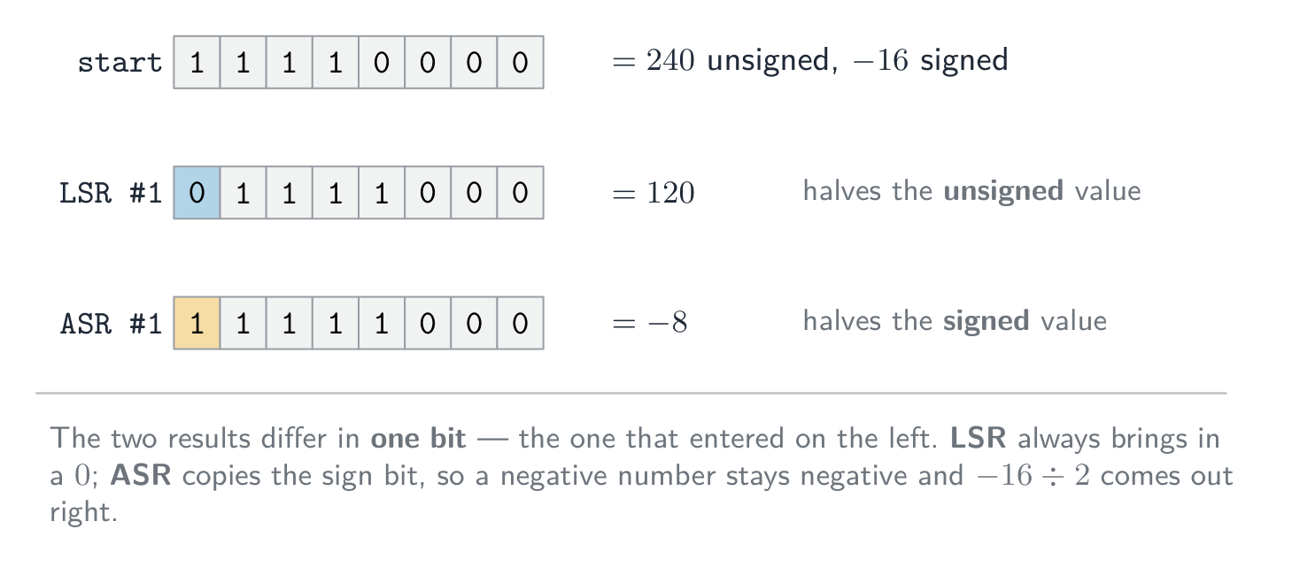
The difference between the two right shifts is a single bit. Take 11110000, which is 240 read as unsigned and $-16$ read as signed. LSR #1 brings in a 0 and gives 01111000 $= 120$, which is the correct half of 240. ASR #1 copies the sign bit instead and gives 11111000 $= -8$, which is the correct half of $-16$. Neither is wrong — each halves the value under one reading.
Bit manipulation for monitoring/control
Embedded devices often use one bit 位 of a register per signal (e.g. bit $n$ = LED $n$). Using a mask 掩码 — bit masking — you can:
- set bit $n$:
R = R ORa mask with bit $n$ set. - clear bit $n$:
R = R ANDa mask with bit $n$ clear and the rest set. - toggle bit $n$:
R = R XORa mask with bit $n$ set. - test bit $n$:
R ANDthe mask, then check if the result is non-zero.

Bit manipulation is fast, uses little memory, and lets one byte hold up to 8 on/off states.
In the exam's instruction set these are AND, OR and XOR with a mask written as a denary, binary or hexadecimal operand. With the ACC holding 10101100:
| Instruction | Mask | Result in ACC | Effect |
|---|---|---|---|
AND B00001111 |
00001111 |
00001100 |
keeps only the low four bits (clears the others) |
OR #1 |
00000001 |
10101101 |
sets the least significant bit, leaving the rest unchanged |
XOR &FF |
11111111 |
01010011 |
inverts every bit |
AND B00001000 then CMP #0 |
00001000 |
00001000 |
tests bit 3: the compare is not equal, so bit 3 was set |
LSL #2 |
10110000 |
shifts left two places, losing the top two bits | |
LSR #3 |
00010101 |
shifts right three places, zeros entering on the left |
"Write the instruction that sets the least significant bit to 1 and leaves the others unchanged": OR #1, or OR B00000001. To clear a bit use AND with a mask that has a 0 in that place and 1s elsewhere; to test a bit, AND with a mask that has a 1 only in that place, then compare the result with zero. In a monitoring device, one bit of a register per sensor lets a single AND check whether a particular sensor is on, and one OR switches an actuator's control bit on without disturbing the others.
Explore
Shift and mask the bits of a byte
Pick an operator and watch each result bit. A left shift (<<) moves every bit up one place (×2); a right shift (>>) moves them down (÷2); AND with a mask clears the bits you don't want.
Vocabulary
Train
| English | Chinese | Pinyin |
|---|---|---|
| logical shift | 逻辑移位 | luó jí yí wèi |
| cyclic shift | 循环移位 | xún huán yí wèi |
| bit | 位 | wèi |
| mask | 掩码 | yǎn mǎ |
4.3
Definitions the examiner accepts
A definition question is marked against fixed wording. Learn these exactly, and give one answer only.
| Term | Definition |
|---|---|
| stored program concept | the program instructions and the data are both held in main memory, and instructions are fetched and executed one at a time |
| register | a small, very fast storage location inside the processor with a specific purpose |
| Program Counter | the register holding the address of the next instruction to be fetched |
| Memory Address Register | the register holding the address of the memory location being read from or written to |
| Memory Data Register | the register holding the data or instruction just read from, or about to be written to, memory |
| Current Instruction Register | the register holding the instruction currently being decoded and executed |
| Accumulator | the general-purpose register holding the result of the last arithmetic or logic operation |
| cache memory | small, fast memory close to the processor holding frequently used instructions and data |
| interrupt | a signal from a device or program that causes the processor to pause the current task and run an interrupt service routine |
| assembly language | a low-level language in which each mnemonic instruction corresponds to one machine-code instruction |
| immediate addressing | the operand is the value written in the instruction |
| direct addressing | the operand is the contents of the address written in the instruction |
| indirect addressing | the address in the instruction holds the address of the operand |
| indexed addressing | the operand's address is the address in the instruction plus the contents of the index register |
| relative addressing | the operand's address is given as an offset from the address of the current instruction |
| logical shift | every bit moves the given number of places and zeros fill the vacated places |
4.3
Exam tips
- Learn the fetch-execute cycle in register-transfer terms (PC, MAR, MDR, CIR, ACC) and what increments the PC.
- Name each register's job; the address bus is one-way, the data bus is two-way.
- Distinguish the addressing modes (immediate, direct, indirect, indexed) — a frequent question.
- Explain how clock speed, number of cores, cache size and word length affect performance.
- For a binary shift, state whether it is logical or arithmetic; a left shift multiplies by 2, a right shift divides by 2.
Common mistakes
- Saying the PC holds the current instruction, or the MDR holds an address. The PC holds the address of the next instruction; the MDR holds data or an instruction, never an address.
- Leaving the increment of the PC out of the fetch, or putting it after the execute. It happens as soon as the address has been copied to the MAR.
- Reading
LDD 10as "load 10".LDD 10loads the contents of address 10;LDM #10loads the number 10. - Putting a value in the ACC column for
CMPorOUT. A compare sets a flag only; an output goes to the output column. - Saying an interrupt is handled "immediately". The processor finishes the current instruction and checks for interrupts at the end of the cycle.
- Using a logical right shift on a negative two's-complement number. Only an arithmetic shift keeps the sign bit.
Interactive lessons on this topic
Work through it step by step, with instant-check exercises.
A-Level Computer Science Past Papers